SSD Controller | SATA NAND Flash Controller
Secure and Reliable Low Power SATA Controller for the IIoT and Demanding Applications- Designed to fully satisfy industrial requirements
- Most power-efficient SATA SSD controller
- 32-Bit dual-core microprocessor with optimized instruction set and additional hardware accelerators for flash memory handling
- hyMap® customizable sub-page-based Flash Translation Layer
- FlashXE® eXtended Endurance
- hyReliability™ flash management
- Advanced protection against radiation and soft-errors including end-to-end datapath protection, SRAM ECC and low-alpha package
- Custom firmware extensions and feature development through firmware API
- Turnkey solution including firmware, manufacturing kit, test and development hardware, reference schematics, as well as health monitoring tools

X1 Product Information
Target Application
- High reliability & industrial Solid State Drives (SSD)
- Embedded flash storage modules including U.2, M.2, MO-297 and MO-300
- CFast Cards
- System-in-package (SiP) embedded flash drives (eSSD)
- Discrete on-board flash drive or disk-on-board (DoB) integration
Performance
- Sequential read up to 550 MB/s
- Sequential write up to 500 MB/s
- Random write IOPS: 80,000 fresh-out-of-the-box, 20,000 in steady-state (4K)
- Random read IOPS: 40,000
Host Interface & Compliance
- Serial ATA 3.3 compliant
- SATA Gen1 (1.5 Gb/s), Gen2 (3.0 Gb/s) and Gen3 (6.0 Gb/s) transfer speeds supported
- ATA-8 standard compatible
- CFast 2.0 standard compliant
- S.M.A.R.T and health monitoring
- -40 to +85 °C industrial grade version
- SATA slumber and DevSleep support
Controller & CPU
- High performance dual-core microprocessor based on the Hyperstone architecture
- Flexible clock frequency generation through crystal oscillator and PLL
- 16 GPIO pins provide flexibility in the connection of extra logic
- Special GPIO transfer modes include ISO 7816, I2C and SPI
- On-die temperature sensor and support for an optional external sensor
- Automatic power-down mode during wait periods for host data or flash memory operation completion, automatic sleep mode during host inactivity periods
- Real-time-clock (RTC)
- End-to-end (E2E) datapath protection
- SRAM ECC
- TCG Opal Support
- Performant AES-128 and AES-256 support with CBC and XTS modes
- Random number generator
- SHA-256 Hashing engine
- Secure-Boot features
- Low power consumption
Flash Interface
- Supports legacy, Toggle-1/Toggle-2 mode, ONFI NV-DDR and NV-DDR2 NAND
- Two independent flash channels
- Data transfer rate to flash memories up to 400 Mbyte/s on each channel
- Supports up to 16 flash memory chip selects
- Supports up to 16 Kbyte flash page size
- Firmware support for all available flash memory densities: SLC, 3D MLC, 3D TLC and next generation NAND flashes
- Support for pSLC, pMLC mode
- Performant AES-128 and AES-256 support with CBC and XTS modes
- Random number generator
- SHA-256 Hashing engine
- Secure-Boot features
- Flash memory power down logic and flash memory write protect control
- Firmware storage in flash memory, loaded into internal memory by the boot ROM
- FlashXE® encompasses flash characterization, read-channel calibration, advanced ECC algorithms using 1KB to 4KB code-words and soft-decoding, read-retry and RAID features to ensure the lowest possible read error rates
Flash Memory Management
- HyReliability™ flash management: superior wear leveling, read disturb management and power fail management to ensure the highest reliability and endurance
- hyMap® customizable sub-page-based Flash Translation Layer (FTL) mapping enables second to none random write performance, minimal write amplification, and consequently the highest endurance for usage profiles with emphasis on random access (e.g. JEDEC Enterprise)
- Flexible pre-format settings for SLC caching, over-provisioning, RAID protection and performance tuning
- Advanced thermal management features to maximize performance and data protection at extended temperatures
- Optimized for fast boot-up times
- Static, Dynamic and Global Wear leveling to maximize system write endurance
- Bad Block Management
- Intelligent Garbage Collection
- Read Disturb Management and Dynamic Data Refresh to maximize data retention
- Management of sudden power-fails
- Interleaving, cache, and multi-plane programming
- Firmware is stored redundantly for recovery and refresh
- In-Field Firmware update without user data loss
- Secure erase, fast erase and secure TRIM
- Custom firmware extensions and feature development through firmware API including advanced security support and smartcard chip enablement
- Customized firmware, optimizations and feature implementations possible upon request
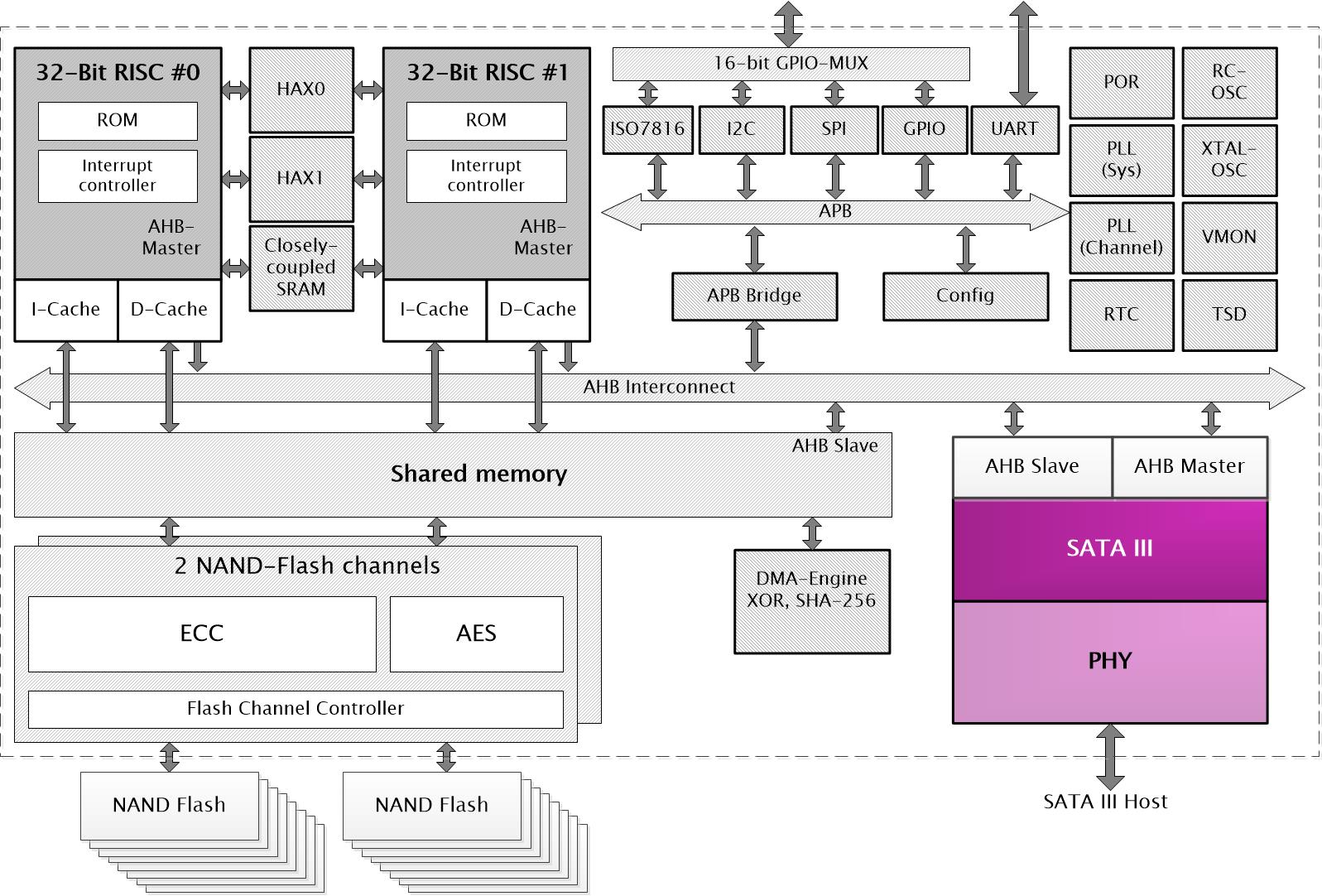
Block Diagram

Order Information
- X1-RAB07 (TFBGA-144, 10.4 x 10.4 x 1.2 mm, 16 CEs, RoHS, -40 to +85 °C)
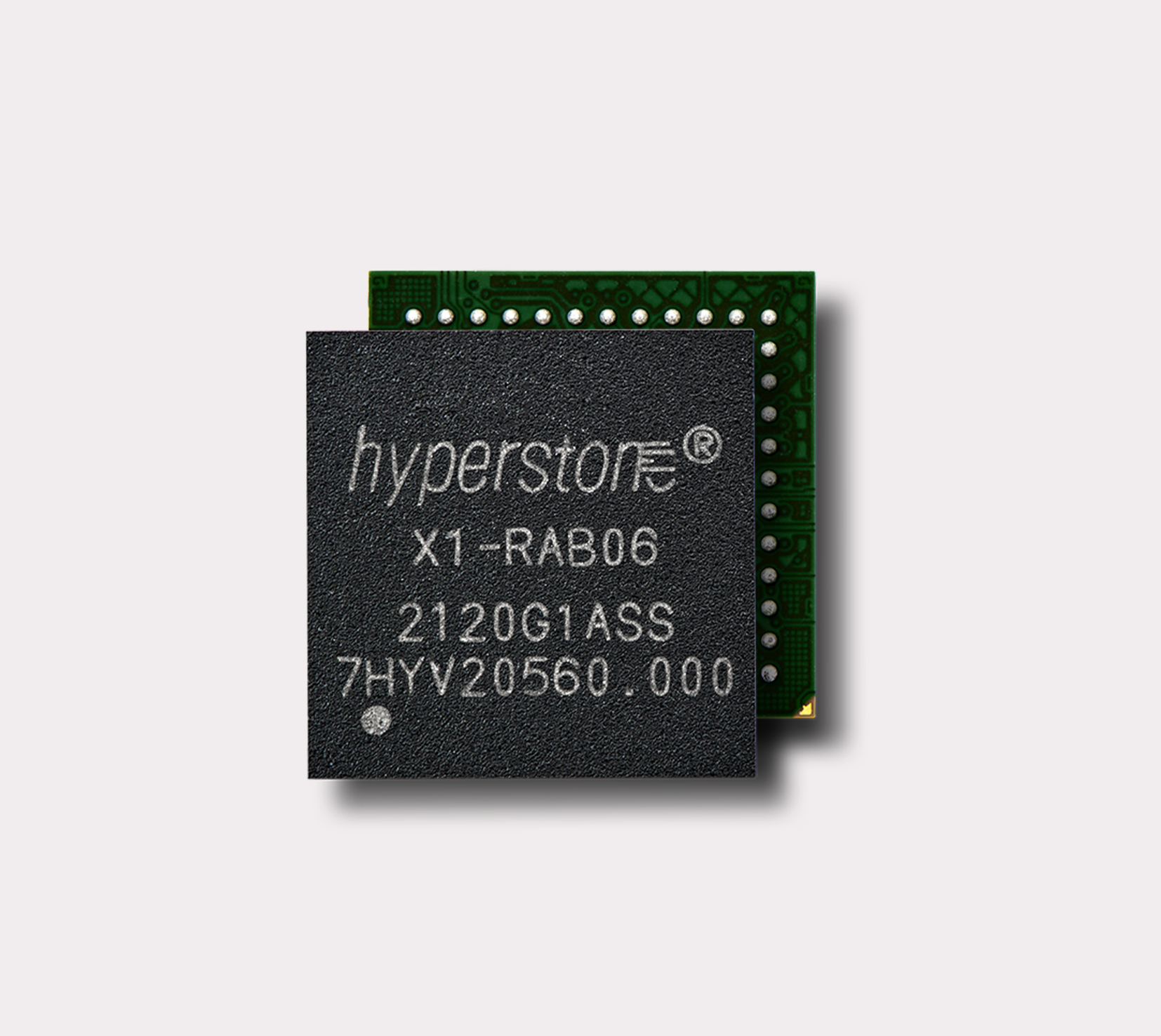
- X1-RAB06 (TFBGA-124, 9 x 9 x 1.2 mm, 16 CEs, RoHS, -40 to +85 °C)
- X1-LAB06 (TFBGA-124, 9 x 9 x 1.2 mm, 8 CEs, RoHS, 0 to +70 °C)
- X1-0ABD0 (Probed Die, 16 CEs, RoHS, -40 to +85 °C)
Email us Today!
Get in touch today for inquiries and support.
Call us Today!
Our team is ready to answer your questions.


