U8 | USB 2.0 NAND Flash Controller
Reliable USB 2.0 NAND Flash Controller for Industrial grade USB Flash Drives, eUSB Modules, MCPs & DoB Storage SolutionsThe Hyperstone U8 family of flash memory controllers together with provided application and flash specific firmware offers an easy-to-use turnkey platform for industrial, high endurance robust flash memory cards or modules compatible to host systems with USB 2.0 interface.
- Designed to satisfy industrial requirements
- hyReliability™ Flash Management
- hyMap® Flash Translation Layer and mapping
- Continuously updated Flash Memory chip support and long term availability
- Flexible 96-Bit/1K BCH ECC engine supporting all Flash Memory requirements
- Optimized 32-Bit RISC core, instruction set for Flash Memory handling
- High performance on-the-fly AES 128 and 256 encryption engine
- Custom features can be implemented with simple firmware upgrades
- Turnkey solution including firmware, manufacturing kit, test and development hardware, as well as reference schematics

Additional U8 Product Information
Target Application
- Industrial USB Flash Drive
- eUSB, embedded USB module
- Ultra durable Flash Drive
- Security Flash Drive
- Multi-Chip-Package (MCP)
- Disk-on-Board
Performance
- Host transfer rate of up to 480 MBit/s
- Sequential read and write up to 35 MB/s
Host Interface & Compliance
- Fully compliant to USB 2.0 specifications
- USB mass storage device class (MSC)
- USB human interface device class (HID) support is possible
- 4 configurable endpoints
- Hi-speed and Full-speed mode possible
- Bulk, isochronous, and interrupt transfer modes
- S.M.A.R.T. and Secure Erase support using ATA pass through
- Configurable Early-Acknowledge
Controller & CPU
- High performance 32-Bit Hyperstone RISC microprocessor
- Large internal RAM provides firmware flexibility
- Unique ID for security applications
- AES encryption engine 128 and 256-Bit
- High performance on-the-fly encryption/decryption
- Flexible clock frequency generation through internal oscillator and PLL
- Automatic power down mode during wait periods for host data of Flash Memory operation completion, automatic sleep mode during host inactivity periods
- Supply voltage 3.3V ± 5%
- Application Programming Interface (API) and Software Development Kit (SDK)
Flash Memory & Interface Handling
- Direct Flash Memory Access (DFA) co-processor including page buffers and interleaving capability
- Synchronous DDR interface compliant with Toggle DDR and ONFI 2.3, compatible with all DDR Flash Memory devices
- Asynchronous SDR interface, ONFI 1.0 compliant, compatible with all legacy interface Flashes
- Data transfer rate to Flash up to 200 MB/s
- Flexible 96-Bit/1K BCH ECC engine
- CRC for additional reliability
- Direct connection of up to 4 Flash Memory chip enables (CE)
- Flash memory power down logic and Flash Memory write protect control
- Supporting all Flash technologies and all page sizes up to 16 KB
- On-chip voltage regulator for 1.8V Flash Memory I/O power
Flash Memory Management
- hyReliability™ Flash Memory Management optimizing reliability, power fail safety, endurance, data retention, and performance
- Complete Flash Translation Layer (FTL) for random Flash data access including mapping of logical block addresses (LBA) to physical block addresses (PBA)
- Bad Block Management
- Static and Global Wear leveling to maximize write endurance
- Inherent on-the-fly garbage collection
- Read Disturb Management, dynamic data refresh to maximize data retention and refresh data subject to read disturbance
- Management of sudden power-fails
- Interleaving, cache, and multi-plane programming
- Firmware is stored redundantly for recovery and refresh
- In-Field Firmware update without user data loss
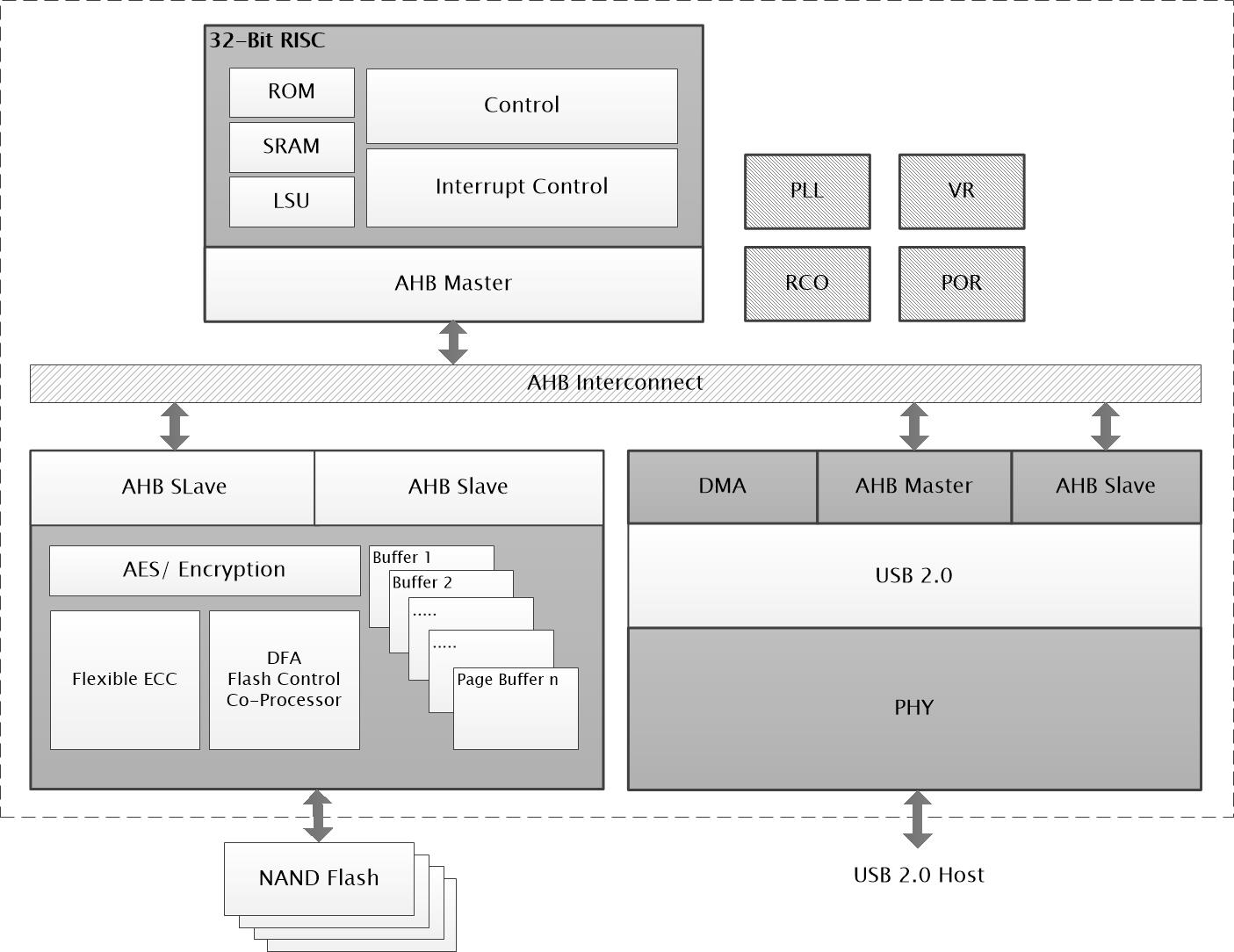
Block Diagram

Order Information
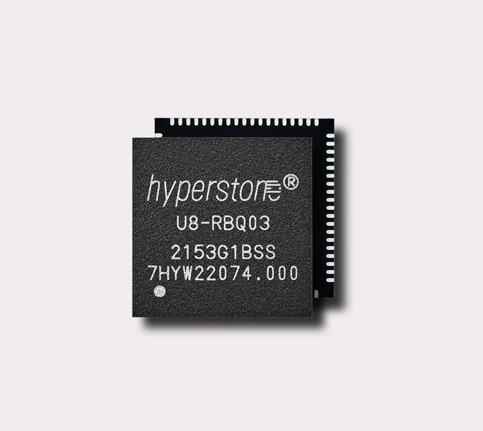
- U8-RBQ03 (QFN 76, 9.0 x 9.0 x 0.9mm, 4 CEs, RoHS, -40 to +85 °C)
- U8-RB1Q03 (QFN 76, 9.0 x 9.0 x 0.9mm, 4 CEs, RoHS, -40 to +85 °C)
Email us Today!
Get in touch today for inquiries and support.
Call us Today!
Our team is ready to answer your questions.

