USB 3.1 NAND Flash Memory Controller
Reliable USB 3.1 NAND Flash Memory Controller for Industrial grade USB Flash Drives & eUSB ModulesThe Hyperstone U9 NAND Flash Controller offers an easy-to-use turnkey solution for industrial, high endurance, and robust Flash Memory drives or modules compatible to host systems with USB 3.1 SuperSpeed 5 Gbps interface.
- Designed to fully satisfy industrial requirements and feature requirements
- hyReliability™ Flash Management including superior wear leveling, read disturb management, and power fail management
- hyMap® Flash Translation Layer and mapping offering second to none random write performance, minimal write amplification, and consequently highest endurance for random access heavy usage profiles (e.g. JEDEC Enterprise)
- Flexible 96-Bit/1K BCH ECC engine supporting all Flash Memory requirements
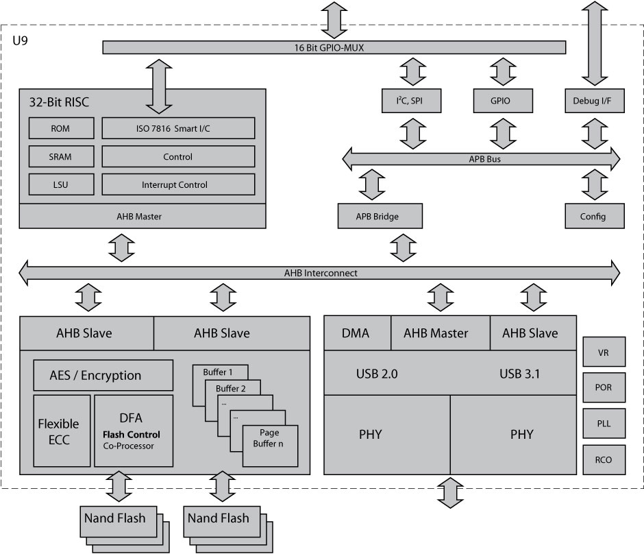
- Optimized 32-Bit RISC core, instruction set for Flash Memory handling
- High performance on-the-fly AES 128 and 256 encryption engine
- 16 GPIOs for customer specific applications supporting SPI, I2C and ISO7816 or additional flash CE
- Built-in temperature sensing capability

U9 Product Information
Target Application
- Industrial USB Flash Drive
- eUSB, embedded USB module
- Ultra durable Flash Drive
- Security Flash Drive
- Multi-Chip-Package (MCP)
- Disk-on-Board
Performance
- Fully compliant with USB 3.1 Gen 1 specifications
- USB mass storage device class (MSC)
- USB Attached SCSI (UASP) support
- SuperSpeed, High-Speed, Full-Speed
- Host transfer rate of up to 5 Gbps
- Sequential read up to 200 MB/s
- Sequential write up to 150 MB/s
- Sustained 4K random write over 5 MB/s
- Secure Erase and Sanitize support
- S.M.A.R.T. and health monitoring
- -40 to +85 °C industrial grade version
Host Interface & Compliance
- Compliant to USB 3.1 Gen1
- USB mass storage device class (MSC)
- USB human interface device class (HID) support is possible
- 4 configurable endpoints
- Supporting Full-Speed, Hi-Speed and SuperSpeed 5Gbps transmissions
- Bulk, isochronous, and interrupt transfer modes
- USB Attached SCSI (UASP) support
- S.M.A.R.T. Sanitize, and Secure Erase support using ATA pass through command
- Configurable Early-Acknowledge to avoid any data loss during power fail
Controller & CPU
- High performance 32-Bit Hyperstone RISC microprocessor
- Large internal RAM provides firmware flexibility
- 16 GPIO pins for customer specific applications, multiplexed interface options include: 16 GPIO, SPI, I2C, 8x CE and ISO7816
- NTC thermistor interface and ADC for high accuracy temperature logging and optimized read/write operations
- Unique ID for security applications
- AES-128 and AES-256 support with CBC and XTS modes, high performance on-the-fly encryption/decryption
- Hardware RNG
- Flexible clock frequency generation through internal oscillator and PLL
- Automatic power-down mode during wait periods for host data or Flash Memory operation completion, automatic sleep mode during host inactivity periods
- On-chip switching voltage regulator for 1.2V controller core power
- Supply voltage 3.3V ± 5%
- Application Programming Interface (API) and Software Development Kit (SDK)
Flash Memory & Interface Handling
- Direct Flash Memory Access (DFA) co-processor incl. page buffers and interleaving capability
- DDR interface compliant with Toggle DDR and ONFI 2.3, compatible with all DDR Flash Memory devices
- Asynchronous SDR interface, ONFI 1.0 compliant compatible with all legacy interface Flashes
- 2-Channels with data transfer rate to Flash up to 200 MB/s each
- Flexible 96-Bit/1K BCH ECC engine supporting all Flashes
- CRC for additional reliability
- Connection of up to 16 Flash Memory chip enables (CE, including 8 GPIO CEs)
- Flash Memory power down logic and write protect control
- Supporting all Flash technologies and all page sizes up to 16KB
- On-chip voltage regulator for 1.8V Flash Memory I/O power
Flash Memory Management
- hyReliability™ Flash Memory Management optimizing reliability, power fail safety, endurance, data retention, and performance
- hyMap® Flash Translation Layer offering class-leading random write performance, minimal write amplification, and highest endurance for random usage profiles (e.g. JEDEC Enterprise)
- Complete Flash Translation Layer (FTL) for random Flash data access including mapping of logical block addresses (LBA) to physical block addresses (PBA)
- Bad Block Management
- Static, Dynamic and Global Wear leveling to maximize write endurance
- Intelligent garbage collection
- Read Disturb Management, dynamic data refresh to maximize data retention and refresh data subject to read disturbance
- Management of sudden power-fails
- Interleaving, cache, and multi-plane programming
- Firmware is stored redundantly for recovery and refresh
- In-Field Firmware update without user data loss
- Customized firmware, optimizations and feature implementations possible upon request.
Block Diagram

Order Information
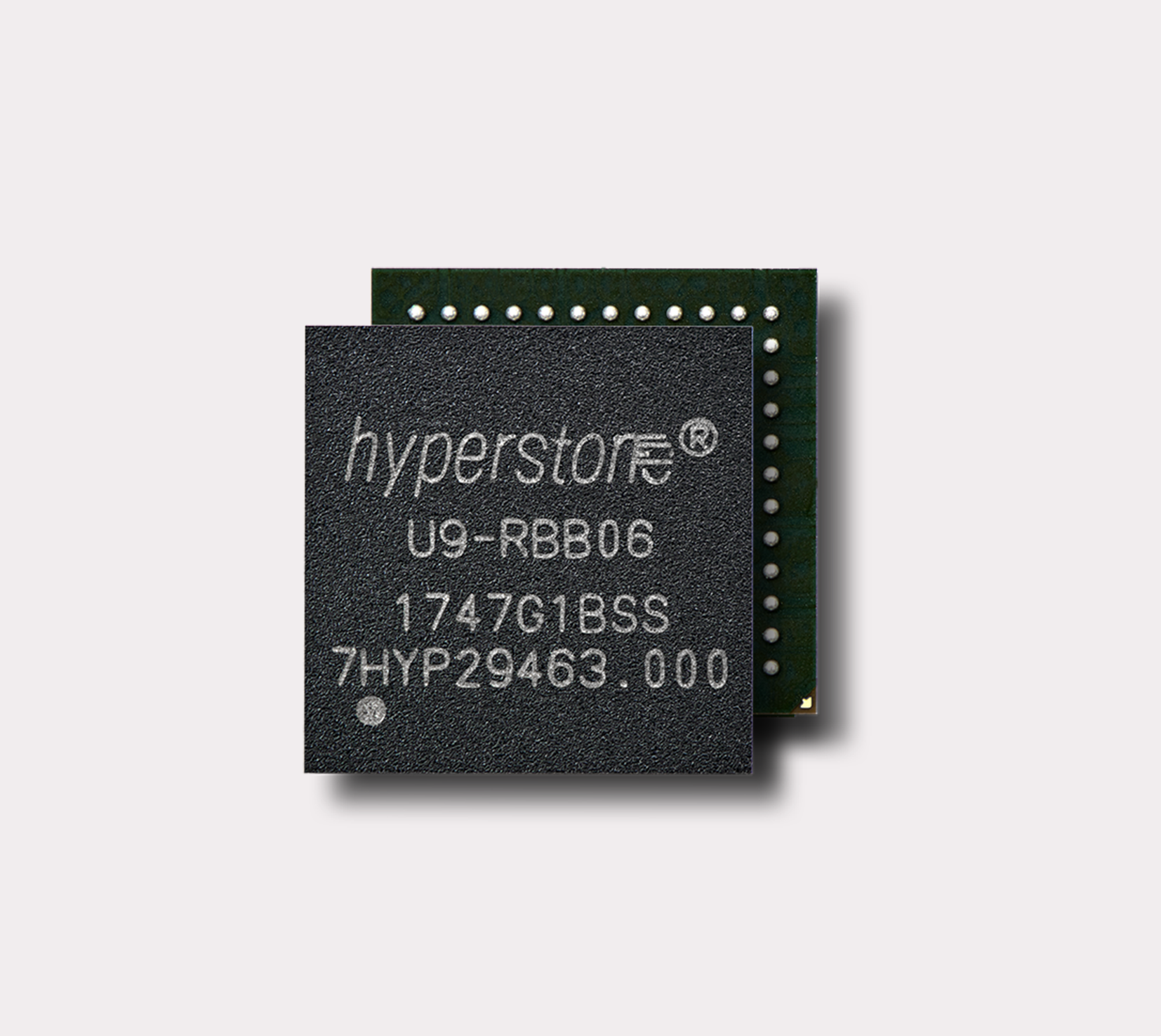
- U9-RBB06 (TFBGA-124, 9x9x1.2mm, 8 CEs, RoHS, -40 to +85 °C, tape-and-reel)
- U9-RBB06-Y (TFBGA-124, 9x9x1.2mm, 8 CEs, RoHS, -40 to +85 °C, tray)
- U9-0BBD0 (Tested Die / Wafer)
Email us Today!
Get in touch today for inquiries and support.
Call us Today!
Our team is ready to answer your questions.


